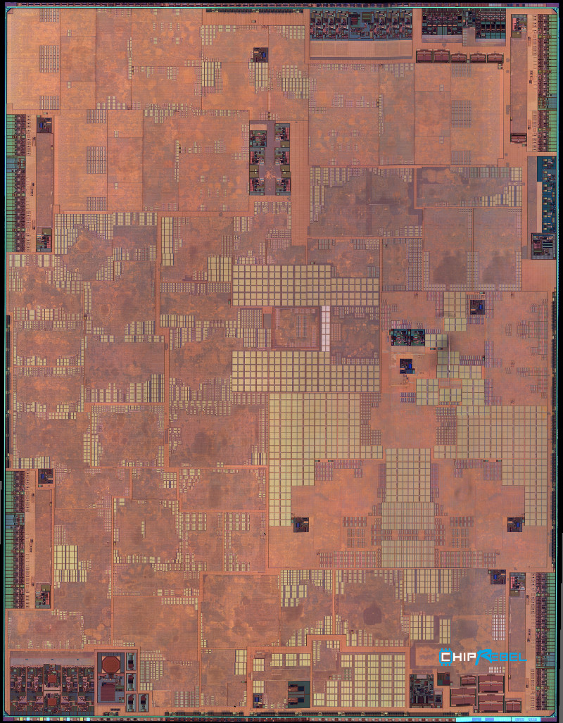
Apple’s newest SoC is build on the 10nm FinFET process of TSMC. It has a 64-bit architecture and it delivers a new neural net to support smooth FaceID. It contains a custom GPU designed by Apple itself. There is an embedded ISP (Image Signal Processing) unit which is used to process data from the 12MP camera. It contains 2 high performance cores (Monsoon) for the ‘real deal’ and four high-efficiency cores (Mistral) for background tasks to maintain battery life. When required it put all six of them to work simultaneously.
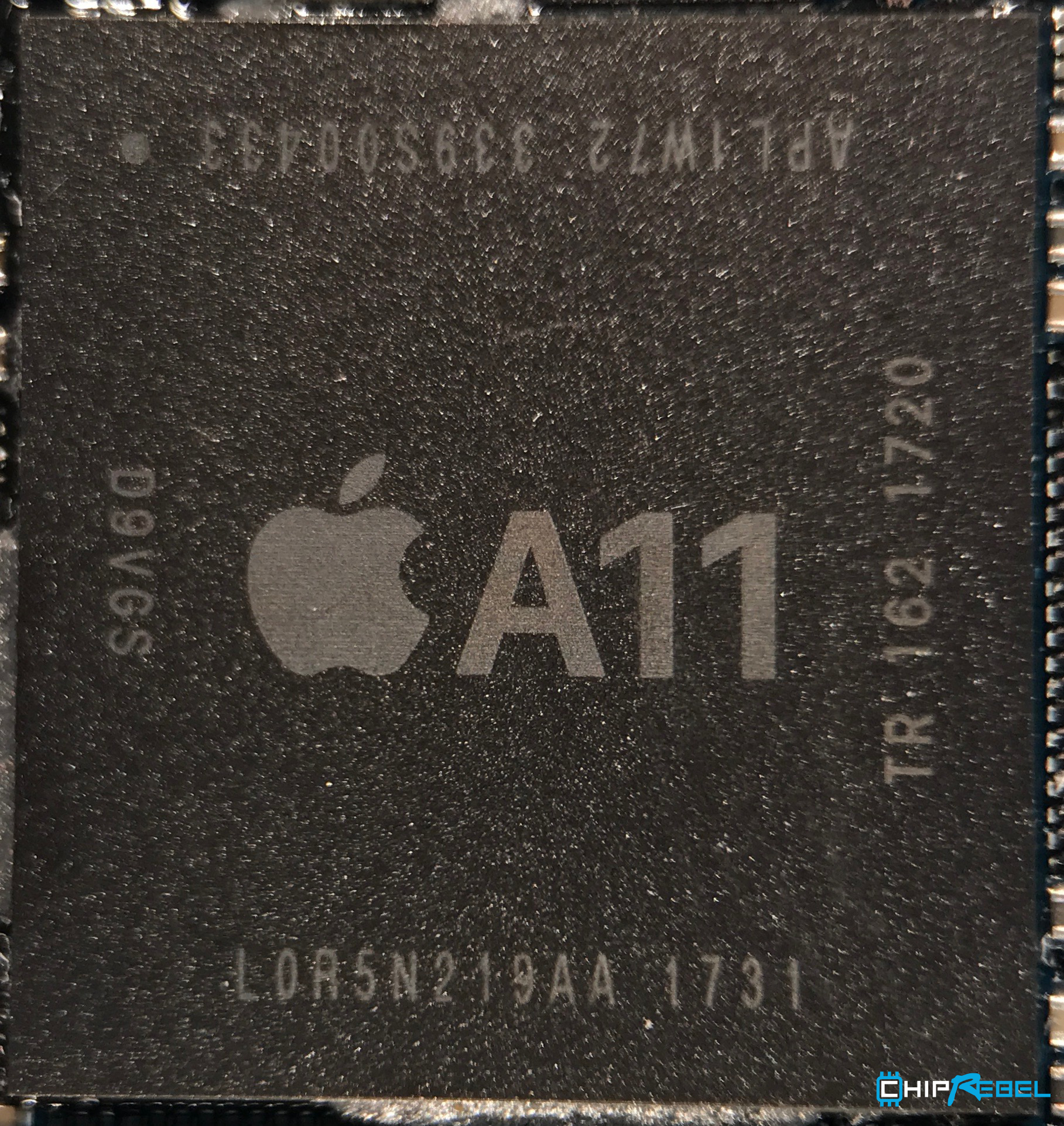
Okay let’s get to work. We’ve teared down the iPhone 8 and reviewed the mainboard containing the A11 Bionic SoC. The iPhone 8 model A1905 we had in our hand contained a A11 Bionic processor with productcode APL1W72 339S00433 (see teardown article). It is manufactured in a Package-on-Package (PoP) with four memory chips stacked.
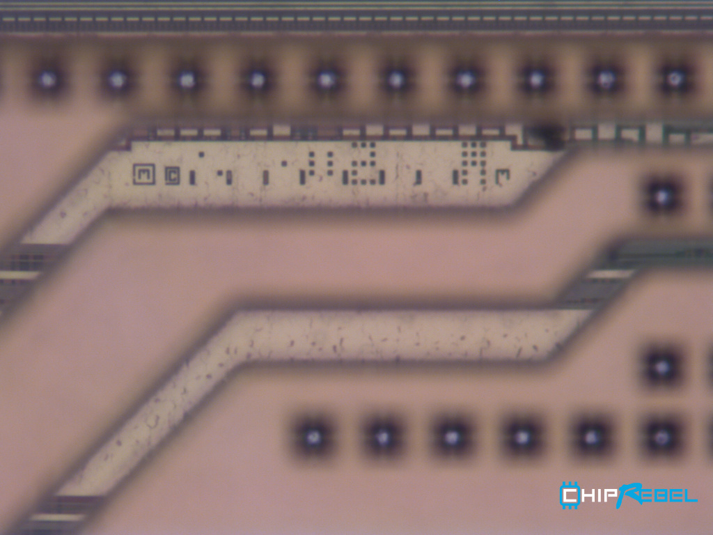
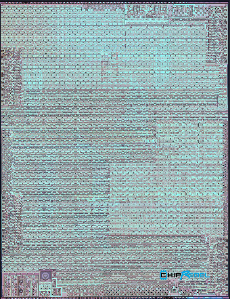
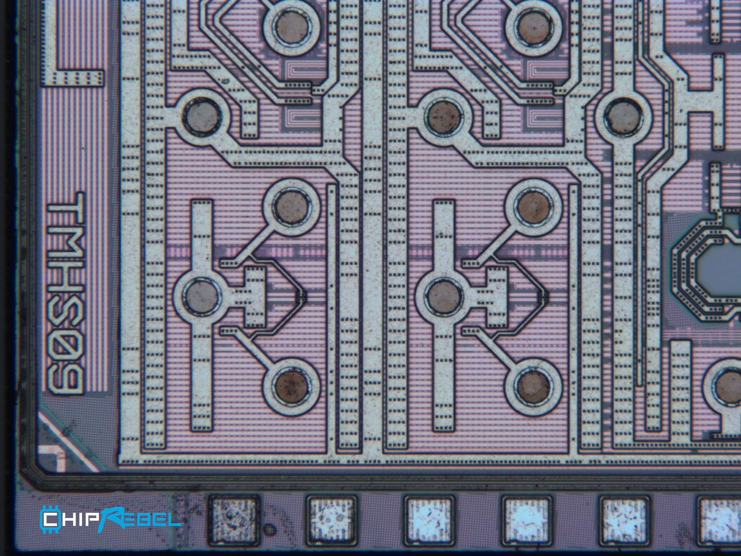
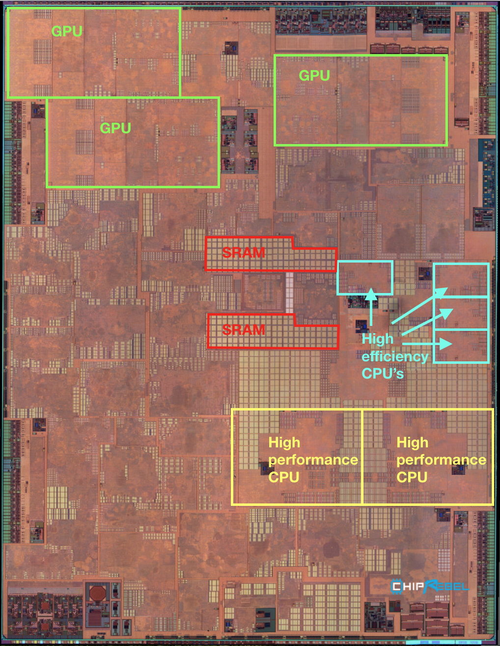
We’ve extracted the die from the PoP. It has a 8197 x 10674 µm die size an a thickness of 160 µm. Click here for big 300ppi floorplan frontside die photo with 50% introduction discount. We had a closer look at the die marking and can confirm it is ‘ TMHS09 ‘
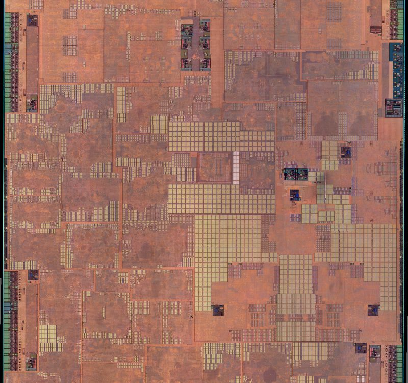
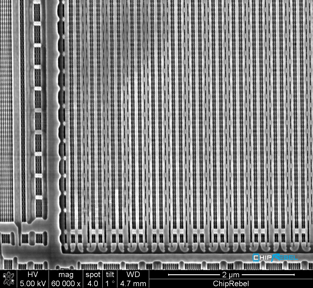
From the backside we have made an optical image floorplan and some Scanning Electron Microscopy (SEM) images.
A11 Bionic layout chip backside view. Image is horizontal flipped to match Frontside view
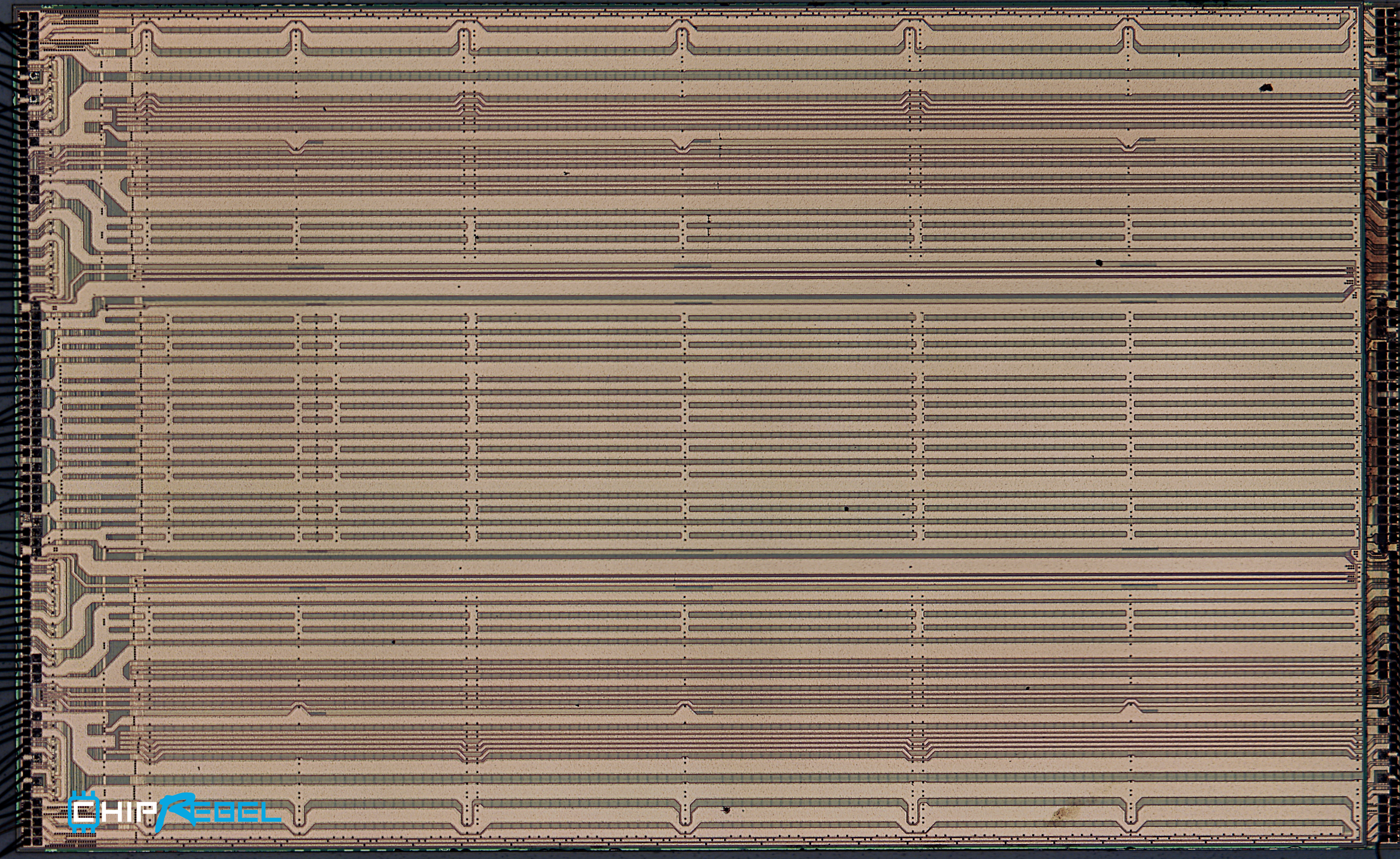
The iPhone 8 version A1905 would have a 2GB of RAM integrated in the A11. We have found four stacked memory chips on top of Apple’s TMHS09 silicon die which implies they contain 500 MB of RAM memory cells each. Images shown below confirms it contains the LPDDR4 RAM chips of Micron.